Modern products of microelectromechanical systems (MEMS) meet high requirements in terms of reliability of compounds of dielectric materials, in particular special-purpose products. Nowadays mechanical and welding ways are applied for such compounds in the process of forming MEMS structures and integrated circuits’ (IC) arrangement at the stages of assembly and installation into the housing. The first group comprises compounds with the application of special retainers, glued or soldered joints. The second method includes welding of materials, sprayed over the surface of dielectrics, and high-frequency welding.
Mechanical methods are not technologically efficient and group, which results in increased costs of articles. They often don’t let get compounds which meet reliability requirements, especially for small-size articles and special-purpose ones. Direct high-frequency welding of dielectric materials without auxiliary layers requires careful consideration of process parameters both for each welded dielectric individually and for their combination in accordance with factors of dielectric material losses. It significantly complicates technological process and increases the total cost of articles.
Dielectric compound can also be achieved by welding of materials sprayed on their surface. Such compounds are not very reliable because in this case the criterion is the level of the adhesion of the film of the sprayed material to the surface of joint dielectrics. The depth of diffusion of the film material into the dielectric will be no more than 1-2 atomic layers which is enough to achieve good adhesion of the film to the dielectric surface but not enough to provide a reliable connection of two dielectric substrates.
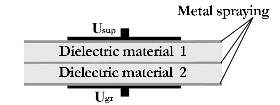
As an alternative to existing methods the Department of “Micro- and nanoelectronics” has offered a new way of dielectric materials’ welding. Its purpose is deep diffusion of metal coating, sprayed on the surface of one of the samples, into joint dielectric materials. Diffusion in the place of contact of joint materials is conducted by the transfer of metal coating particles into dielectric materials under the influence of a strong electrical field. For this welding is performed in two stages with the change of polarity of starting electrodes.
Department №27 employees have conducted a research of process of welding of two ceramized plates by the developed method. Metal aluminum coating has been used with the thickness of nearly 100 nm sprayed at the surface of plate by magnetron sputtering.
The conducted research has shown the advantages of the developed method: possibility to weld small-size samples (2x2 mm), compactness of the welded compound (welded connection does not exceed the thickness of metal coating), the reliability of the compound is raised because of the diffusion depth. Moreover, new technology is simple and group.
Below: a schematic diagram of dielectric materials’ welding.